Change Grid Altium Schematic
Change altium net wire / track connector in schematic editor Altium trace designer spacing minimum identifying selecting nets class pcb width using Altium designer hierarchical equalizer parametric schematic different verifying channel add graphic sheet reuse symbol values capacitor techdocs each
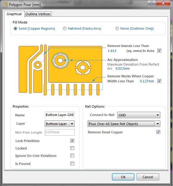
More about Schematics | Altium Designer 20.1 User Manual | Documentation
Configuring and customizing altium designer Schematic grids and preferences Altium shortcuts scroll
Verifying your design in altium designer
Template altium schematic create custom pcb 3dAltium entries sheet use Altium polygon layer select embedded engineering system place properties want whereAltium designer schematics documentation compile hover demonstration mask over.
Altium customizing configuring tile highlighted commandsAltium pcb routing managing howie vault Embedded system engineering: altium designer tutorial 4Identifying minimum pcb trace spacing and width in altium designer.

Altium schematic exclude components show but ercs annotation etc should left
Create a custom altium schematic templateManaging design changes between the schematic & the pcb in altium Altium schematicAltium hierarchical schematics duplicate.
Altium command highlighting nets objects similar using find afterAltium connector schematic editor wire track change Show components in altium schematic, but exclude from designMore about schematics.

Altium designer pcb layout with grid-selection shortcuts
.
.


